
Compute Chips
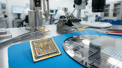
ASIC vs. GPU in 2026: Broadcom’s Custom Silicon Order Book Reveals the Shift
The AI chip market is becoming more diverse, not simply replacing one processor with another. GPUs remain valuable for programmable computing, while large customers increasingly commission custom accelerators that reflect their own workloads, infrastructure, and economics.
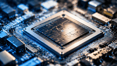
OpenAI’s Custom Chip with TSMC: The First Major LLM Company Going Silicon
OpenAI is moving deeper into the hardware beneath its models. Instead of relying exclusively on processors designed for a broad market, it is helping create silicon around the workloads that power its own products. That is a significant change in responsibility: the company is no longer only a customer of computing infrastructure, but also a participant in defining it.

Inference Era Pricing: Why LPU Architecture Targets the Token Generation Bottleneck
The price of an AI response depends on more than how much arithmetic a chip can perform. It depends on how quickly the system accesses data, how efficiently it schedules requests, and whether the resulting answer arrives within the application’s time limit.

China’s TPU Breakthrough: How Zhonghao Xinying Filled the Pure TPU Architecture Gap
China’s AI chip industry is often discussed through GPUs and neural-processing units. Zhonghao Xinying offers another route: a processor designed around tensor computation, supported by its own instruction set and computing platform.

More Threads and Biren’s GPU Iteration Race: China’s General-Purpose AI Compute Path
China’s domestic AI hardware effort is not following one architectural route. Some companies emphasize specialized neural processors. Others are pursuing programmable GPUs that can support a broader mix of training, inference, and general computing workloads.

Nvidia’s $1 Trillion Revenue Target by 2027: Behind the AI Factory Transformation
Nvidia’s trillion-dollar ambition is not a forecast of $1 trillion in revenue during the single year 2027. It is a statement about the cumulative business opportunity associated with Blackwell and Vera Rubin through that period—and about the scale of infrastructure customers may need as AI moves into continuous operation.
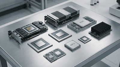
Vera Rubin Platform Breakdown: 7 Chips, 5 Racks, and a 10x Inference Efficiency Leap
Nvidia’s Vera Rubin platform is easiest to understand as a coordinated AI infrastructure system, not simply a new GPU surrounded by accessories. Its components divide responsibility across computation, networking, storage, and orchestration so that fewer resources sit idle while another part of the system becomes a bottleneck.

Nvidia’s Groq 3 LPU: The Inference Coprocessor That Could Reshape AI Server Architecture
For years, the AI infrastructure conversation has revolved around a familiar question: how many GPUs can a data center deploy? Nvidia’s Groq 3 LPU suggests that the next question may be more interesting: which parts of an AI workload should actually run on those GPUs?

Liquid Cooling for 1000W+ AI Chips: The Infrastructure Bottleneck Nobody Priced In
The accelerator arrives. The server vendor has completed its work. The software team is ready to begin testing. Then the deployment stalls because the building cannot remove enough heat.

AI Chip Yield Challenges at 3nm: The Cost of Advanced Node Scaling
A smaller manufacturing node promises more computing capability within a constrained footprint. For AI chips, that can mean additional arithmetic units, improved energy efficiency, or room for functions that would be difficult to accommodate on an older process. The attraction is obvious. The economics are less automatic.

TPU 8t Commercial Launch: Can Google’s Custom Silicon Finally Challenge Nvidia’s Moat
Google’s TPU 8t can challenge Nvidia in selected large-scale AI workloads, but it does not need to replace GPUs everywhere to matter. Its strongest opportunity is to make Google’s infrastructure an attractive alternative for customers willing to optimize models and software around a different computing platform.
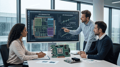
Custom Silicon for Inference: Why Hyperscalers Are Designing Their Own LPUs
The economics of AI change when a model moves from development into daily use. Training attracts attention because it requires spectacular computing resources. Inference creates the recurring bill: every search, generated answer, recommendation, and coding suggestion consumes computing capacity.

The Post-Moore Path for AI Chips: Advanced Packaging Succeeds Process Scaling
For decades, the semiconductor industry rode a remarkably simple storyline: shrink transistors, pack more of them onto a die, and enjoy automatic gains in performance and efficiency. That story—embodied in Moore’s Law—still matters, but for AI chips in the mid‑2020s it is no longer the sole, or even primary, driver of progress.

Global AI Accelerator Market Breaks $250B in 2026: A Supply Chain Teardown
By 2026, AI accelerators have moved from niche hardware to the beating heart of modern compute, powering everything from frontier model training to real‑time inference across clouds, enterprises, and edge devices. Crossing the $250 billion mark in annual market value is not just a milestone; it is a reflection of a vast, intricate supply chain that stretches from design labs and fabs to packaging houses, board makers, system integrators, and the services that wrap around them. Understanding how this value is created and captured requires a teardown of the AI accelerator supply chain, layer by layer.

AI Chip TDP Grows 50% Per Gen, Data Center Power Architecture Faces Reassessment
Over the past several AI chip generations, one trend has become impossible to ignore: thermal design power (TDP) is climbing at a pace that would have seemed extreme even a few years ago. When flagship accelerators and high‑end AI chips see TDP grow on the order of 50% per generation, the consequences extend far beyond chip packaging.

Practical Breakthroughs of Domestic EDA Tools in AI Chip Design (Huada/Prime)
As AI chips surge to the forefront of national technology strategies, attention has increasingly turned from fabs and packaging to a crucial but less visible layer: electronic design automation (EDA). For many years, domestic EDA tools lagged behind international leaders, limiting how far local firms could push advanced AI chip design without external dependencies.

Analyzing the Optimal Balance Between R&D Expense Ratio and Market Share for AI Chip Firms
AI chip companies sit at the center of one of the most capital‑intensive and innovation‑driven industries in the world. Their success depends on sustained, heavy investment in research and development, yet they must also deliver financial performance that satisfies investors, funds next‑generation fabs and packaging, and supports competitive pricing. The question of how much to spend on R&D—expressed as an R&D expense ratio relative to revenue—cannot be answered in isolation.

Competitive Landscape of AI Chip IP Licensing Models (ARM/RISC-V)
As AI chips move from niche accelerators to pervasive compute foundations in data centers, edge devices, and embedded systems, the way CPU and AI cores are licensed has become a strategic question rather than a mere technical detail. ARM’s established commercial IP licensing model and the rising ecosystem around RISC-V represent two contrasting philosophies: one offers mature, standardized cores under proprietary licenses;

FCF Inflection Point Forecasting Model for Leading AI Chip Companies
As AI chip companies mature from high‑growth stories into capital‑intensive platforms, investors increasingly focus on free cash flow (FCF) as the core signal of long‑term value creation. Revenue growth, unit shipments, and benchmark leadership still matter, but they no longer tell the full economic story. What ultimately determines whether a leading AI chip company justifies its valuation is when, and how, its investments in R&D, tape‑outs, capacity, and ecosystem translate into sustained, positive, and growing FCF. This transition moment is what we can call the FCF reflection point.

The Threat of In-House Chips: Deep Dive on Google TPU v7 vs. Amazon Trainium 3
The AI hardware landscape in 2026 is defined not just by traditional semiconductor vendors, but increasingly by hyperscalers building their own, deeply integrated silicon. Among the most important examples are Google’s TPU v7 and Amazon’s Trainium 3, two generations of in‑house accelerators aimed squarely at large‑scale AI training and inference in their respective clouds.

Die-to-Die Interconnect (UCIe/BoW) Breaks Multi-Chip Module Performance Bottlenecks
For years, multi‑chip modules (MCMs) and chiplet‑based designs have promised a way around the limits of monolithic system‑on‑chips: better yield, more flexible integration, and modular reuse of IP. Yet one constraint kept their potential in check—the performance bottlenecks at the interfaces between dies. As long as die‑to‑die links behaved more like “mini‑PCIE slots” than true on‑chip fabric, MCMs could not fully match the speed and efficiency of large single dies.

Interpreting the Surge in Secondary Market Trading Volume for AI Chips
The rapid rise of AI has created unprecedented demand for high‑end accelerators, from data‑center GPUs to custom AI chips and complete inference boards. As supply challenges, long lead times, and aggressive deployment plans collide, a secondary market for AI chips has emerged and grown dramatically.

The CoWoS Capacity Allocation Game: Who Gets a Bigger Slice from TSMC?
In the mid‑2020s, one of the most strategic bottlenecks in the global AI hardware ecosystem is not just advanced logic wafer capacity, but advanced packaging capacity—and in particular, TSMC’s CoWoS (Chip‑on‑Wafer‑on‑Substrate) lines. As AI accelerators, high‑bandwidth memory (HBM) stacks, and multi‑die systems proliferate, securing a larger slice of CoWoS capacity has become a competitive game played by the world’s largest chip and cloud companies.

Liquid Cooling Transitions from Optional to Mandatory, Supply Chain Demand Surges
For years, liquid cooling sat on the fringe of mainstream data center design: a powerful but complex option reserved for the most extreme high‑performance systems. Today, that status is changing. As AI accelerators, dense GPUs, and specialized compute ASICs drive rack power far beyond traditional envelopes, liquid cooling is making a decisive transition from “nice to have” to “mandatory” in a growing share of deployments.

Long-Term Replacement Threat of Quantum Computing to AI Chips: Timing and Path
Every major technology wave eventually faces the question of succession: what comes after it, and when? AI chips—GPUs, TPUs, custom accelerators—have defined the current era of machine intelligence by enabling massive parallel computation on classical hardware. Quantum computing, with its radically different model of information processing, is often cast as a long‑term replacement threat to these AI chips. The reality is more nuanced.

Nvidia B200 vs. AMD MI400: The 2026 AI Chip Crown Battle
By 2026, the race to power large‑scale artificial intelligence has crystallized into a few headline contests, and one of the most closely watched is the emerging battle between Nvidia’s B200 platform and AMD’s MI400 series. Both families target the same high‑stakes arena: training and inference for frontier‑scale models, hyperscale data centers, and enterprise AI deployments that push compute, memory, and networking to their limits.

2026 Changes in Government AI Chip Procurement Lists: Enhanced Security & Trust Requirements
By 2026, government procurement and approval processes for AI chips have shifted from a narrow focus on performance and basic compliance to a broader, more demanding emphasis on security, trust, and lifecycle assurance. Procedure lists that once concentrated on technical specifications, testing protocols, and documentation now embed deeper requirements around supply chain transparency, hardware security features, and verifiable trustworthiness of both silicon and software.

Thermal Simulation Challenges and Solutions in 3DIC AI Chip Design
As AI workloads push chips to deliver ever higher compute density, designers are increasingly turning to three‑dimensional integration (3DIC) to stack dies vertically and pack more functionality into limited footprints. While 3DIC architectures unlock significant performance and bandwidth advantages, they also introduce complex thermal behaviors that are far harder to predict and manage than in traditional 2D layouts.

Commercialization Progress of Neuromorphic Chips: 2026 Application Scenario Validation
Neuromorphic chips have occupied a fascinating space in the semiconductor and AI worlds for more than a decade: rich in promise, modest in revenue, and frequently described as “five years away” from mainstream adoption. By 2026, however, the conversation has shifted. While neuromorphic hardware is still far from displacing GPUs or general‑purpose accelerators, we now see concrete application scenarios where these chips are moving out of labs and pilot projects and into commercial trials, edge products, and specialized services.

2026 AI Chip ASP Trends: Price Pressure Testing After Supply Ramp-Up
Average selling prices (ASP) of AI chips surged through the early waves of the generative AI boom, driven by scarcity, steep performance requirements, and aggressive infrastructure build‑outs. As we move through 2026, however, the story shifts: supply has ramped up across leading‑edge nodes, packaging, and memory, and the market has entered a phase where price pressure is actively testing just how resilient those elevated ASPs really are.

Training Chip Growth Slows, Inference Chips Take the Growth Baton
For several years, AI infrastructure investment has been dominated by a single narrative: build ever‑larger clusters of training accelerators to push the frontier of model size and capability. Capital poured into high‑end GPUs and specialized training chips, and the industry’s growth story revolved around headline figures for compute‑days and parameter counts. Now the center of gravity is starting to shift.

Edge AI NPU Penetration in AI PCs and Smartphones Exceeds 40%
As edge artificial intelligence has shifted from novelty to necessity, one metric captures the depth of that change: neural processing unit (NPU) penetration in client devices. When more than 40% of newly shipped AI PCs and smartphones include dedicated NPUs, it signals a structural transition in how compute is architected at the edge.

Investment Insights from Hot Chips 2026 on the 2027 AI Chip Technology Roadmap
By mid‑2026, the AI hardware world has learned to treat Hot Chips not just as a technical conference, but as an unofficial preview of the next year’s capital flows. Architectures unveiled, packaging roadmaps hinted at, and memory strategies debated on stage all feed into how investors think about the 2027 AI chip landscape. When engineers share their plans, markets quietly rearrange expectations.

Sustainability of AI Chip Stock Valuations: A Dual PEG and P/S Test
AI chip companies have become the market darlings of the mid‑2020s, with valuations that often seem to defy traditional metrics. Price‑to‑earnings ratios climb, price‑to‑sales multiples stretch, and investors debate whether the surge reflects a durable structural shift or a bubble waiting to deflate. In this environment, assessing the sustainability of AI chip stock valuations demands more than a single metric.

Silicon Photonics (CPO) Penetration Acceleration Curve in AI Cluster Optical Interconnects
As AI clusters scale to tens of thousands of accelerators and beyond, the limitations of traditional electrical interconnects become increasingly apparent. Bandwidth demands, reach requirements, and power constraints push data center architects to seek new ways to move bits efficiently between nodes. Silicon photonics, and in particular co‑packaged optics (CPO), has emerged as a critical technology for addressing these challenges.

The Cost-Benefit of GPU Cluster Migration from InfiniBand to Ethernet (RoCE)
As AI training clusters scale from dozens to thousands of GPUs, the interconnect fabric becomes one of the largest and most strategic line items in the infrastructure budget. For years, InfiniBand has been the de facto choice for high‑performance GPU clusters, particularly in large‑scale deep learning and HPC environments. At the same time, Ethernet with RDMA over Converged Ethernet (RoCE) has quietly matured, closing much of the performance gap while retaining the economic and operational advantages of mainstream Ethernet ecosystems.

Impact of Upgraded Reliability and Lifetime Test Standards on AI Chip Yields
As AI workloads move from experimental deployments to mission‑critical services, expectations around the reliability and lifetime of AI chips have risen sharply. Data centers, automotive systems, industrial controllers, and consumer devices now run AI models continuously, often under harsh thermal and electrical conditions. In response, chip makers and system integrators are upgrading reliability and lifetime test standards to ensure their devices can withstand years of heavy duty.

China’s AI Chip Localization: The Qualitative Leap from "Usable" to "Good"
Over the past decade, China’s push to localize its semiconductor stack has moved from an aspirational policy goal to an operational reality, especially in the realm of AI chips. Early domestic accelerators were often labeled “good enough” or merely “useful” – serviceable for certain workloads, but rarely the first choice for cutting‑edge model training or large‑scale deployment. Today, the conversation is shifting.

ASICs Eating into GPU Share: Broadcom and Marvell’s Golden Era
For much of the last decade, GPUs have been the default answer to almost any question about high‑performance compute and AI acceleration. They offered flexible parallelism, strong software ecosystems, and a simple story: one architecture, many workloads. That narrative is starting to fragment. In more data‑center racks and custom systems, application‑specific integrated circuits (ASICs) are quietly claiming sockets that might once have gone to GPUs.

AI Inference Chip Landscape: Startups Challenging Nvidia’s Triton Ecosystem
AI inference has quietly become the backbone of modern digital experiences: search, recommendation, content ranking, copilots, and vision systems all depend on running trained models efficiently and at scale. In this realm, Nvidia’s Triton Inference Server and its GPU‑centric ecosystem have established a powerful beachhead, offering a unified way to deploy and manage models across data‑center GPUs. Yet a growing wave of startups is challenging this dominance, not necessarily by duplicating Triton, but by reshaping hardware and software assumptions around inference.

The Profit Erosion Effect of Soaring Tape-Out Costs for China’s AI Chip Designers
In the last few years, China’s AI chip industry has moved from early experimentation to large‑scale commercial deployment, with dozens of design houses racing to tape out increasingly complex accelerators for data centers, edge devices, and vertical applications. At the same time, the cost of moving a design from layout to silicon—tape out—has risen sharply, driven by advanced process nodes, more complex packaging, and growing verification demands.

Tracking Domestic AI Chip Yield Ramp-Up: The Tough Climb from 40% to 70%
When countries or regions commit to building domestic AI chips, they quickly encounter a harsh reality: designing a competitive accelerator is only half the battle. The other half is manufacturing it at scale, with yields high enough to make the economics work. Moving from an early yield of around 40% to a more mature 70% is one of the toughest climbs in semiconductor production.